In this article, we demonstrate how to connect multiple shift registers in-series, focusing on the 74HC595 chip. This method allows us to expand the number of pins we can control from a microcontroller. In the following sections, we’ll also create a library enabling us to control the individual pins of the shift registers.
If you want to learn how the 74HC595 works and how to control it using an Arduino check the article Use 74HC595 Shift Register With Arduino
The code is available on GitHub
Connecting 74HC595 Shift Registers in Series
The 74HC595 shift register has 8 output pins. By connecting two in series, we can double the number of controllable pins. Also, the pins used by the microcontroller to control the shift registers, remains the same (3 pins) regardless of how many 74HC595 are in use. This same principle can be extended to connect multiple shift registers together.
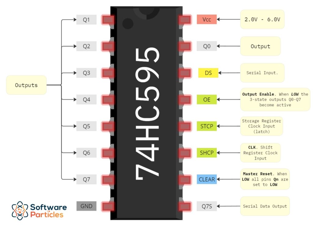
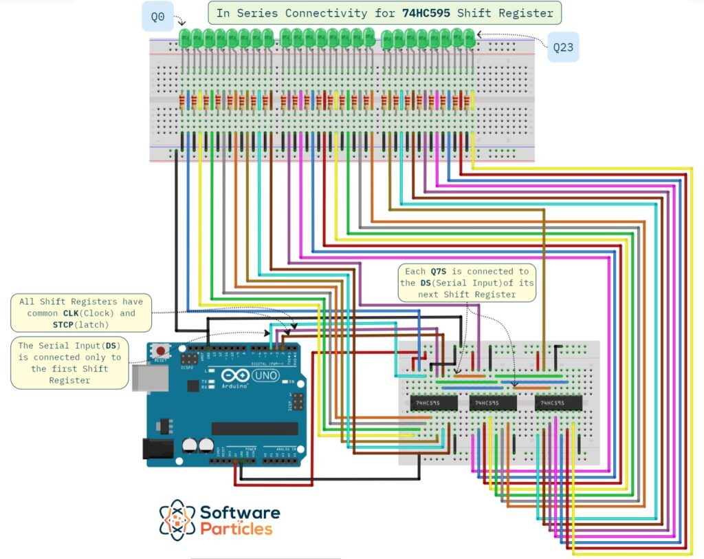
Initially, all shift registers share a common CLK (SHCP or Shift Register Clock Input) and STCP (Storage Register Clock Input or latch). Below is a diagram illustrating the pinout of the 74HC595:
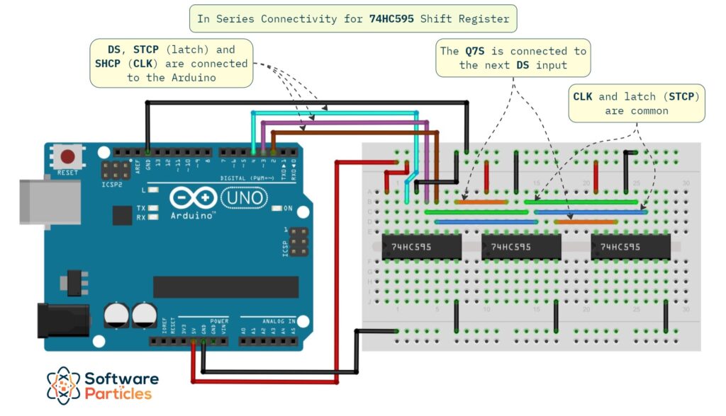
Next, each shift register’s Q7S pin will be connected to the DS (Serial Input) input of the following shift register. The image below demonstrates the connection setup of three 74HC595 shift registers in series, illustrating their shared pins, ground, and Vcc:
For simplicity, the outputs are not displayed here, but they will be shown in illustrations in the next sections.
Transferring Bits from One Shift Register to the Next
While all shift registers in the circuit share common CLK and STCP (latch) pins, the key is to connect the Q7S output from one shift register to the Serial Input (DS) of the next. This enables the transfer of bits from one register to another.
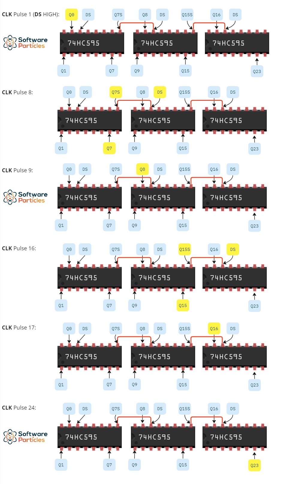
The Q7S output is same as Q7 (with an additional buffer). The overall logic of transferring bits to multiple shift registers is as follows: within 8 pulses of the CLK, a complete transfer of bits occurs to the first shift register. The rest shift registers, will not have any data yet. At the 8th CLK pulse, the Q7S receives its first bit, coming from the 8-bit number transferred into the first shift register. The 9th CLK pulse pulse transfers this bit (from the DS input of the second shift register) into the second shift register. This process continues, allowing the bit to traverse through the shift registers. The results of this mechanism can be observed by executing a simple Arduino sketch that transfers one bit and triggers the clock until it reaches the last output of the last shift register:
// Define pin numbers
#define DS 4    // serialPin
#define STCP 3  // storageRegisterClockPin/latch
#define SHCP 2  // clockPin/CLK

void setup() {
  pinMode(DS, OUTPUT);
  pinMode(STCP, OUTPUT);
  pinMode(SHCP, OUTPUT);
}

void InsertFirstBit() {
  // Set DS high to insert first bit
  digitalWrite(DS, HIGH);
  Clock();
  digitalWrite(DS, LOW);
  Latch();
}

void Clock() {
  // When we set the clock HIGH, the shift register shifts the output by one bit.
  digitalWrite(SHCP, LOW);
  delay(1);
  digitalWrite(SHCP, HIGH);
}

// Flush shift register values to outputs.
void Latch() {
  digitalWrite(STCP, LOW);
  delay(1);
  digitalWrite(STCP, HIGH);
}

void loop() {
  InsertFirstBit();
  delay(500);
  // Trigger clock to fully shift the bit to the end
  // of the 3 shift registers.
  for (int i = 0; i < 23; i++) {
    Clock();
    Latch();
    delay(500);
  }
}
To visualize the Q7S in action, in the following video, a yellow LED is connected to the Q7S output of the first shift register. As we can see, when the Q7 LED of the first shift register is ON, the Q7S (yellow LED) is also ON:
In conclusion, data can be transferred through multiple shift registers, with the first shift register containing a complete byte after the 8th CLK pulse, the second after the 16th pulse, and so on.
To better illustrate the bit transferring process, in the following image, we label the most important outputs of the shift registers, as well as the connections between Q*S and its next DS. Each output highlighted in yellow indicates the presence of the transferred bit at the corresponding clock pulse.
Creating a Library for Controlling Multiple 74HC595 Shift Registers
In this section, we will develop a library to simplify the control of pins across multiple shift registers. To achieve this, we will utilize the SR_74HC595 library, which can control a single shift register. The SR_74HC595 library, makes use of the shiftOut Arduino function for bit transfer. We will build a new component that makes use of the SR_74HC595 library, adding the capability to write a long number and control any pin by its index across an arbitrary number of shift registers.
Arduino and 74HC595 Connectivity Circuit
Below we illustrate the circuit that we will use in this article. The circuit has three 74HC595 shift registers and 24 LEDs connected to their respective outputs.
Additionally, we make use of resistors for the LEDs to limit the voltage, with each resistor having a resistance of 330 Ohms.
Controlling Pins by Writing a Number
One approach for controlling multiple pins is to write a specific binary number to the shift registers. Each output of the shift registers corresponds to a bit of that binary number. For instance, if we wanted to set the Q1 to HIGH and keep all other outputs LOW, we would write the number 2. Similarly, to set Q1 and Q3 to HIGH and the rest to LOW, we would write the number that its binary representation is the following: 00000000 00000000 00001010, which translates to the decimal number 10.
In Arduino UNO, an int takes 2 bytes. A long takes 4 bytes, with a maximum number we can write goes up to 2,147,483,647. 32 bits are plenty in order to control three shift registers, each with 8 bytes.
To write an 8-bit number using the SR_74HC595 library, we can do it as shown below:
#include "SR_74HC595.h"

#define DS 4    // serialPin
#define OE 0    // outputEnablePin, 0 because is not used.
#define STCP 3  // storageRegisterClockPin/latch
#define SHCP 2  // clockPin/CLK

SR_74HC595 SR_74HC595;

void setup() {
  SR_74HC595.init(DS, OE, STCP, SHCP);
  SR_74HC595.enableAutoFlush();

  SR_74HC595.write(105); // 01101001
}

void loop() {}
The above code will produce the following result:
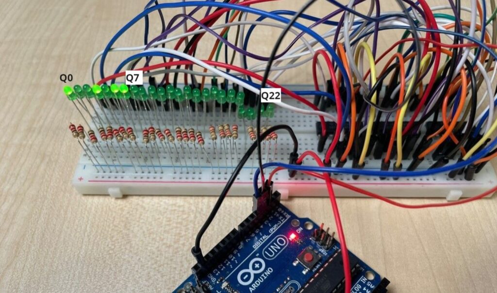
However, if we need to write a number that exceeds 8 bits, we have to break the number into 8-bit chunks (using bitwise operations) and write each one of them separately, since the shiftOut function used, allows only an 8-bit number to be written at a time. This way, when the second byte is written to the Serial Input, the first byte (that we wrote before) continues to shift into the second shift register. Similarly, when the third byte is send through Serial Input, the two previous bytes are shifted one shift register further, until the whole number is transferred. In general, as we write subsequent bytes to the Serial Input, the previously written bytes continue to shift into the subsequent shift registers.
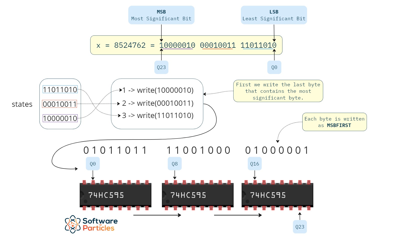
We will create an array called states to store all the bytes, with each byte representing a part of the 32-bit number we want to write. After we create the states array, we write each element to the shift registers using the SR_74HC595 library.
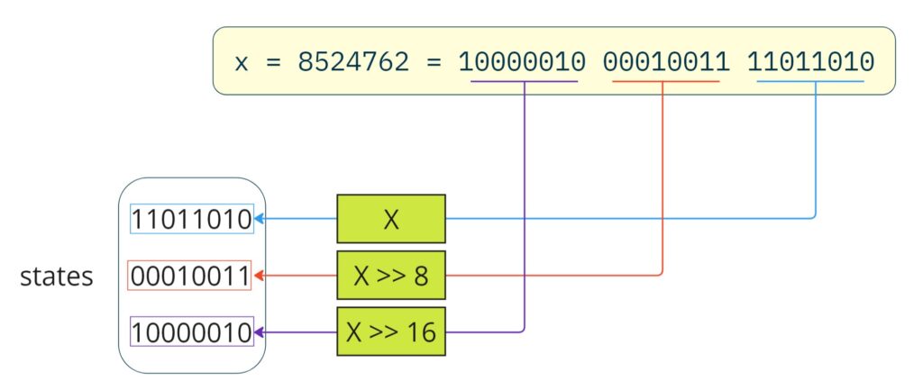
To split a binary number into its bytes, we will use bit operations such as bit shifting (>>). For example, to obtain the second byte of a number, we shift the number 8 bits to the right. Similarly, shifting the number by 16 bits to the right gives us the third byte, and so forth.
The image below show the main logic we use to split the number into bytes/chunks and place each chunk to the states array:
This can be summarized by the following loop, where we set each state array element to the corresponding byte:
for (int i = 0; i < numOfShiftRegisters; i++)
{
   states[i] = value >> 8 * i;
}
Next, we write each element in the states array to the Serial Input (DS). For Most Significant Bit First (MSBFIRST) approach, we begin by writing the last element of the array first, because it contains the most significant byte. This byte, when we write the rest, will be shifted to the last outputs of the shift registers, which represent the most significant bits. This way, we implement a Most Significant Bit First Data Transfer.
To learn more about MSBFIRST and LSBFIRST, you can check out the article Understanding MSBFIRST (Most Significant Bit) and LSBFIRST (Least Significant Bit)
Below, we illustrate how we write each element of the states array to the shift registers. We start by writing the last element first since it holds the most significant byte. This byte is then transferred to the last shift register after the remaining bytes are written. Additionally, each byte is written in MSBFIRST order, making the whole transferring approach to MSBFIRST.
The algorithm for writing the chunks to the Serial Input using the SR_74HC595 library, is shown below:
writeChunks(int *chunks)
{
    SR_74HC595.hold();

    for (int i = _numOfShiftRegisters; i >= 0; i--)
    {
        SR_74HC595.write(chunks[i]);
    }

    if (_enableAutoFlush)
        SR_74HC595.flush();
}
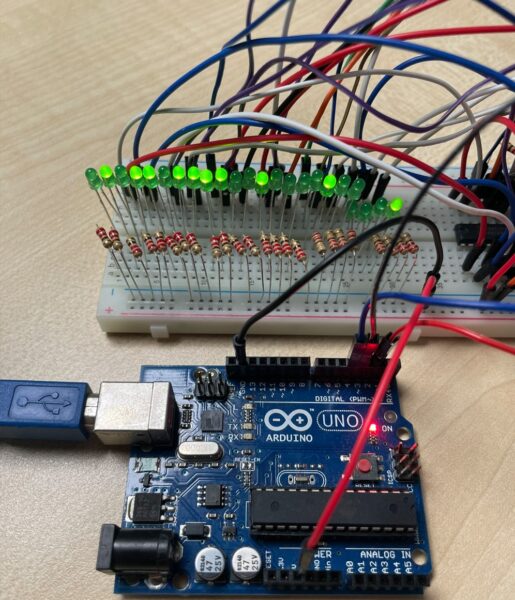
The final result of the code above for writing the number 8524762 (1000 0010 0001 0011 1101 1010), is shown below:
The leftmost bit corresponds to Q0, and the rightmost bit to Q23. The number is written in MSBFIRST order.
Controlling a Specific Pin By Index
In this section, we will explain how we can use the state array and modify the appropriate bit before writing the updated array to the Serial Input.
To begin with, the setPin function will have two parameters: one for the pin index (starting from zero) and another for the pin state (HIGH or LOW). First, we find which array element the pin index belongs to. Then, we modify the specific bit within that array element and set the desired state.
In order to find the array element the pin index belongs to, we can divide the pin index by 8. Since we split the number into bytes, dividing the index by 8 results with the index for the states array. In addition, the modulo of the pin index with 8, gives us the position of the bit we would like to update:
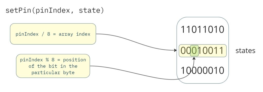
This approach translates to code as shown below:
// The pin is the pin index.
int stateIndex = pin / 8; // We find the index of the states array the pin index belongs to.
int bitposition = pin % 8; // We find the bit position we need to update.
To modify a particular bit within a byte, we can use bit masks. Masks are bytes with specific bits set, and used as operands in bitwise operations. For example, if we want to set the second bit (from the right) of the binary number 01010101 to HIGH (1), then we can use the mask 00000010 and perform a bitwise OR operation. This results in 01010111. This way, we can have masks for each bit position we would like to change. This approach can be summarized in the following code:
if (value == HIGH) // In case we want to set the pin to HIGH.
{
   // From previous step, we have the proper mask.
   states[stateIndex] = states[stateIndex] | mask;
}
Similarly, if we wanted to set the first bit (from the right) of the binary number 01010101 to LOW, we can use the same mask 00000001. First, we invert the bits of the mask resulting to 11111110 and then execute a bitwise AND operation between them. The result will be 01010100. We make the inversion in order to use one array of masks. The code below summarizes this approach:
if (value == LOW)
{
   // From previous step, we have the proper mask.
   states[stateIndex] = states[stateIndex] & ~mask;
}
This way, we can modify a specific bit in the states array, and write the updated chunks to the shift registers.
Putting it All Together: The PinController Library
After learning the various mechanics required to control multiple pins using the 74HC595 Shift Register (applicable to any other Shift Register as well), we bundle all necessary functionality into the PinController library. This library includes an init method for configuring the pins to control the shift registers, a write method with a long number as parameter, and a setPin method to set the state of a specific pin by its index. Below is the PinController.h header file:
class PinController
{
public:
    PinController();

    /*
      DS = serialPin (of first shift register).
      OE = outputEnablePin, 0 if not used.
      STCP = storageRegisterClockPin = latch () (of first shift register)
      SHCP = clockPin = CLK (of first shift register)
    */
    void init(int numOfShiftRegisters, uint8_t serialPin, uint8_t outputEnablePin, uint8_t storageRegisterClockPin, uint8_t clockPin);

    void write(long value);
    void setPin(unsigned int pin, int value);

    void hold();
    void flush();
    void enableAutoFlush();
    void disableAutoFlush();

private:
    SR_74HC595 SR_74HC595;

    int *states;
    int _numOfShiftRegisters;
    bool _enableAutoFlush;

    int masks[8] = {
        B00000001,
        B00000010,
        B00000100,
        B00001000,
        B00010000,
        B00100000,
        B01000000,
        B10000000,
    };

    void initializeShiftRegisters();
    void writeChunks(int *states);
};
The implementation of the write(long value) function in PinController.h first breaks down the number we want to write into bytes, as explained in the previous sections. Then, it calls the writeChunks(int *chunks) function and passes the states array to be written to the Serial Input.
void PinController::write(long value)
{
    for (int i = 0; i < _numOfShiftRegisters; i++)
    {
        states[i] = value >> 8 * i;
    }

    writeChunks(states);
}
The setPin(unsigned int pin, int value) function updates the specific bit we want, identified by its index, with the new state (HIGH or LOW), then calls the writeChunks(int *chunks) with the updated states array, as shown below:
void PinController::setPin(unsigned int pin, int value)
{
    if (pin >= _numOfShiftRegisters * 8)
        return;

    int stateIndex = pin / 8;
    int mask = masks[pin % 8];

    if (value == HIGH)
    {
        states[stateIndex] = states[stateIndex] | mask;
    }
    else if (value == LOW)
    {
        states[stateIndex] = states[stateIndex] & ~mask;
    }

    writeChunks(states);
}
The masks are a property of the PinController header file, as shown below:
int masks[8] = {
   B00000001,
   B00000010,
   B00000100,
   B00001000,
   B00010000,
   B00100000,
   B01000000,
   B10000000,
};
Finally, the writeChunks(int *chunks) function utilizes the write function of the SR_74HC595 library to write the bytes, starting with the last element first, implementing an MSBFIRST approach.
void PinController::writeChunks(int *chunks)
{
    SR_74HC595.hold();

    for (int i = _numOfShiftRegisters; i >= 0; i--)
    {
        SR_74HC595.write(chunks[i]);
    }

    if (_enableAutoFlush)
        SR_74HC595.flush();
}
You can find the complete PinController library on GitHub.
PinController Library Usage Example
In this section, we will demonstrate how to use the PinController library in an Arduino sketch to control 24 pins, which are the outputs of three shift registers connected in series. The sketch assumes the circuit illustrated in the Arduino and 74HC595 Connectivity Circuit section.
We will create a sketch that lights every LED one after the other, from left to right and backwards. To achieve this, we will use two for loops: one incrementing from 0 to 23 and the other from 23 to 0. Additionally, we will use the setPin function of the PinController library to set the current pin to HIGH and set the previous pin to LOW:
#include "PinController.h"

PinController controller;

#define DS 4    // serialPin.
#define OE 0    // outputEnablePin, 0 when not used.
#define STCP 3  // storageRegisterClockPin/latch.
#define SHCP 2  // clockPin/CLK.

void setup() {
  controller.init(3, 4, 0, 3, 2);
  controller.enableAutoFlush();
}

void loop() {
  for (int n = 0; n < 24; n++) {
    controller.setPin(n - 1, LOW);
    controller.setPin(n, HIGH);
    delay(50);
  }

  for (int n = 23; n >= 0; n--) {
    controller.setPin(n + 1, LOW);
    controller.setPin(n, HIGH);
    delay(50);
  }
}
The result of the code above is shown below:


